
Time: 2026.04.22
Published: 2026-04-22 | Industry News
TSMC has officially unveiled its 2026–2027 process and packaging roadmap, introducing next-generation GAA processes (A14/A13/A12), N2U 2nm derivative, and COUPE silicon photonics + CoWoS advanced packaging. The move aims to meet explosive AI data center demand and sustain leadership in advanced nodes.
At the 2026 North America Technology Symposium, TSMC Senior Vice President Kevin Zhang detailed the company’s latest technology blueprint, covering cutting-edge process nodes, advanced packaging, and silicon photonics solutions tailored for AI and high-performance computing (HPC) applications.
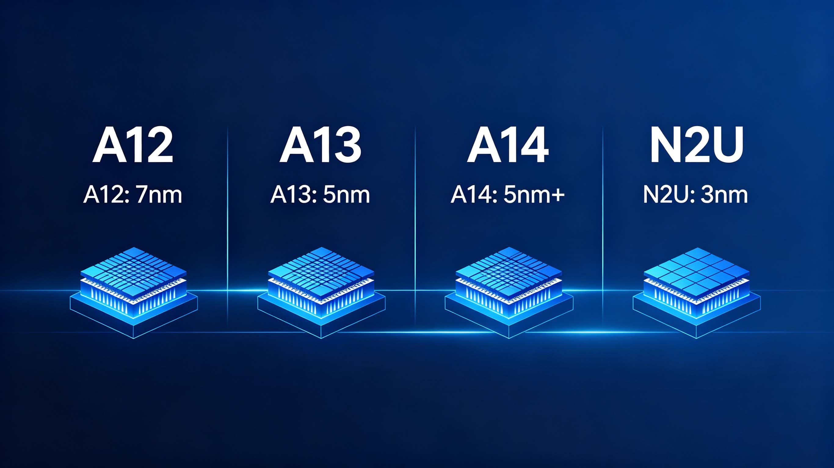
TSMC’s advanced process roadmap through 2029, including A14/A13/A12 and N2U nodes
On the process front, TSMC introduced two derivatives of its 1.4nm gate-all-around (GAA) A14 process—A13 and A12—scheduled for production in 2029. A13 will reduce chip size by approximately 6% compared to A14, maintaining full design-rule compatibility for seamless migration. Additionally, N2U, a power-optimized derivative of the 2nm process, will enter production in 2028, delivering up to 10% power reduction for AI chips.
TSMC projects the global semiconductor market will surpass $1.5 trillion by 2030, with over 55% of revenue driven by high-performance computing and AI. To capture this growth, the company is prioritizing density gains through advanced packaging rather than relying solely on lithography scaling, effectively reviving Moore’s Law via system-level integration.
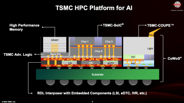
TSMC’s CoWoS advanced packaging and COUPE silicon photonics for AI data centers
A key highlight is the COUPE (Compact Universal Photonics Engine) silicon photonics platform, entering mass production in late 2026. COUPE integrates electrical and photonic dies via SoIC 3D stacking, cutting power consumption by 50%+ and latency by 90% for chip-to-chip interconnects in AI data centers. Paired with CoWoS, it enables 2× lower latency and 2.5× higher power efficiency for AI accelerators.
TSMC is aggressively expanding CoWoS (Chip-on-Wafer-on-Substrate) capacity to address AI demand. Following 5.5× reticle CoWoS (supporting 12 HBM stacks) in 2026, 9.5× reticle CoWoS will launch in 2027, and a 14× reticle version—capable of integrating 10 compute dies and 20 HBM stacks—is slated for 2028. Beyond that, System-on-Wafer (SoW) technology will eliminate substrates, enabling 40× reticle-scale integration by 2029.
Notably, TSMC will delay adoption of ASML’s high-NA EUV tools, instead leveraging multi-patterning on existing low-NA EUV for 2nm and finer nodes. This strategy avoids the $380M+ cost of high-NA tools while sustaining scaling through 2028–2029. However, TSMC lags Intel in backside power delivery, with its Super Power Rail (SPR) tech not arriving until the A16 process in 2027.
Industry analysts view TSMC’s roadmap as a strategic shift to advanced packaging as the primary driver of density gains, complementing GAA processes. With CoWoS capacity constraints easing and COUPE entering production, TSMC is positioned to dominate AI chip manufacturing through 2029, while competitors play catch-up in both process and packaging innovation.